Designing a custom flex sensor
Trill Flex brings flexible touch sensing to your maker projects. Trill Flex comes with a one-axis multitouch sensor printed on flexible PCB, but we designed this sensor to be detachable so you can create entirely custom sensors perfectly suited to your own projects.
In this tutorial we will create a custom 30-button flexible touchpad. You will learn how to set up a KiCad project and include the Trill design files, draw the pads, add a ground plane, and get your design ready to be printed.
Table of contents
- What you’ll learn in this tutorial
- Set up: Download and install KiCad
- 1. Download the KiCad Trill Flex libraries
- 2. Load the trill-flex symbols and footprints
- 3. Set up a new KiCad project
- 4. Add the Trill Flex symbol to the schematic
- 5. Add the Trill Flex footprint to the PCB
- 6. Draw the pads
- 7. Connect the nets
- 8. Make the connections
- 9. Draw an outline
- 10. Run the design rules and electrical check
- 11. Generate the file for manufacturing
- 12. Get your sensor ready to use!
What you’ll learn in this tutorial
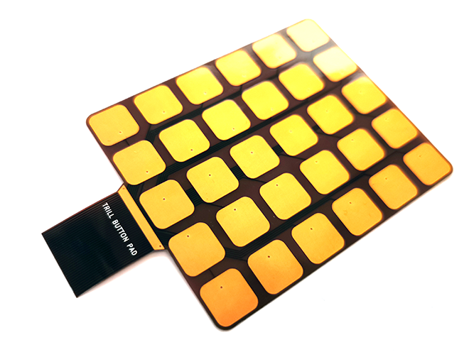
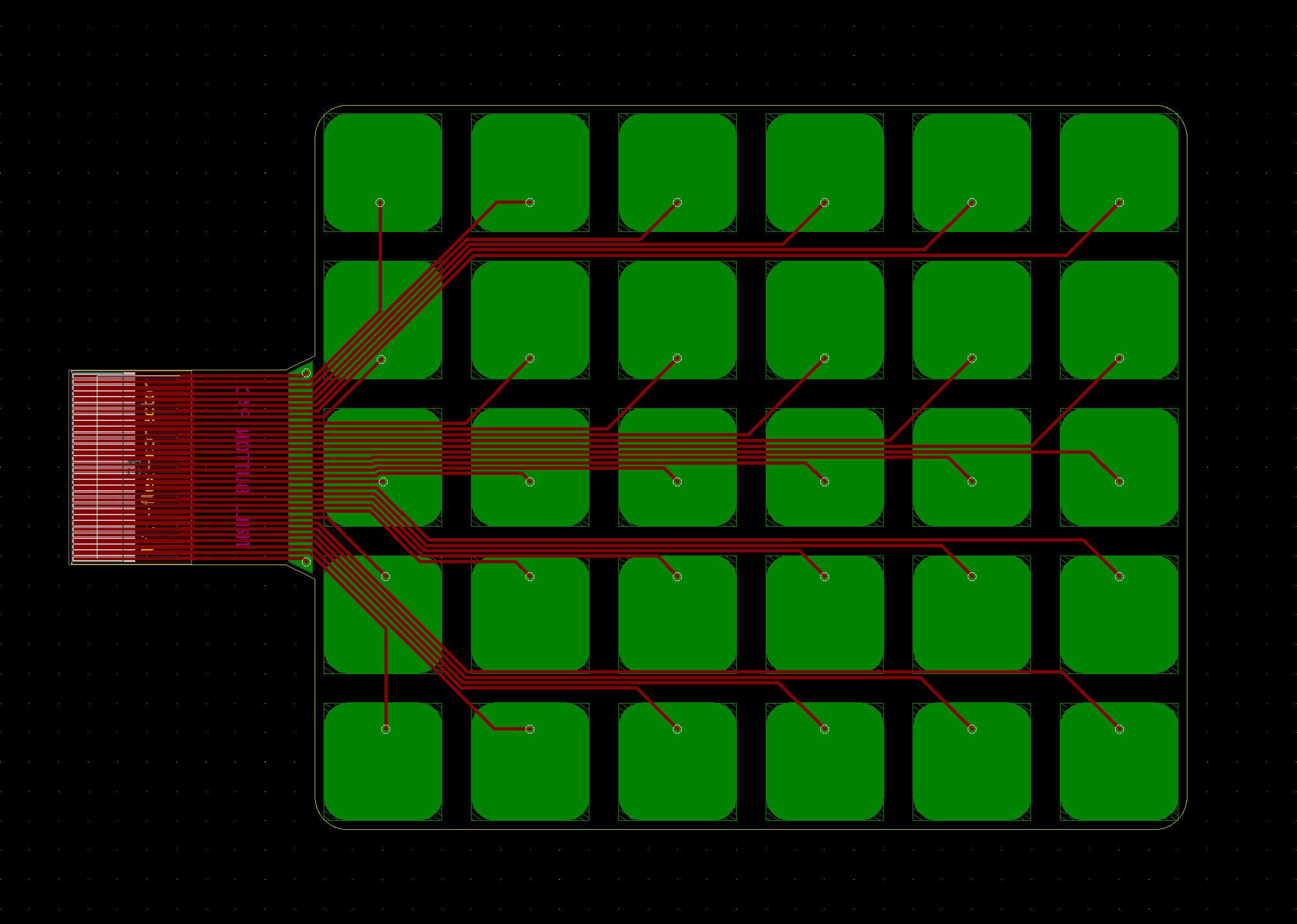
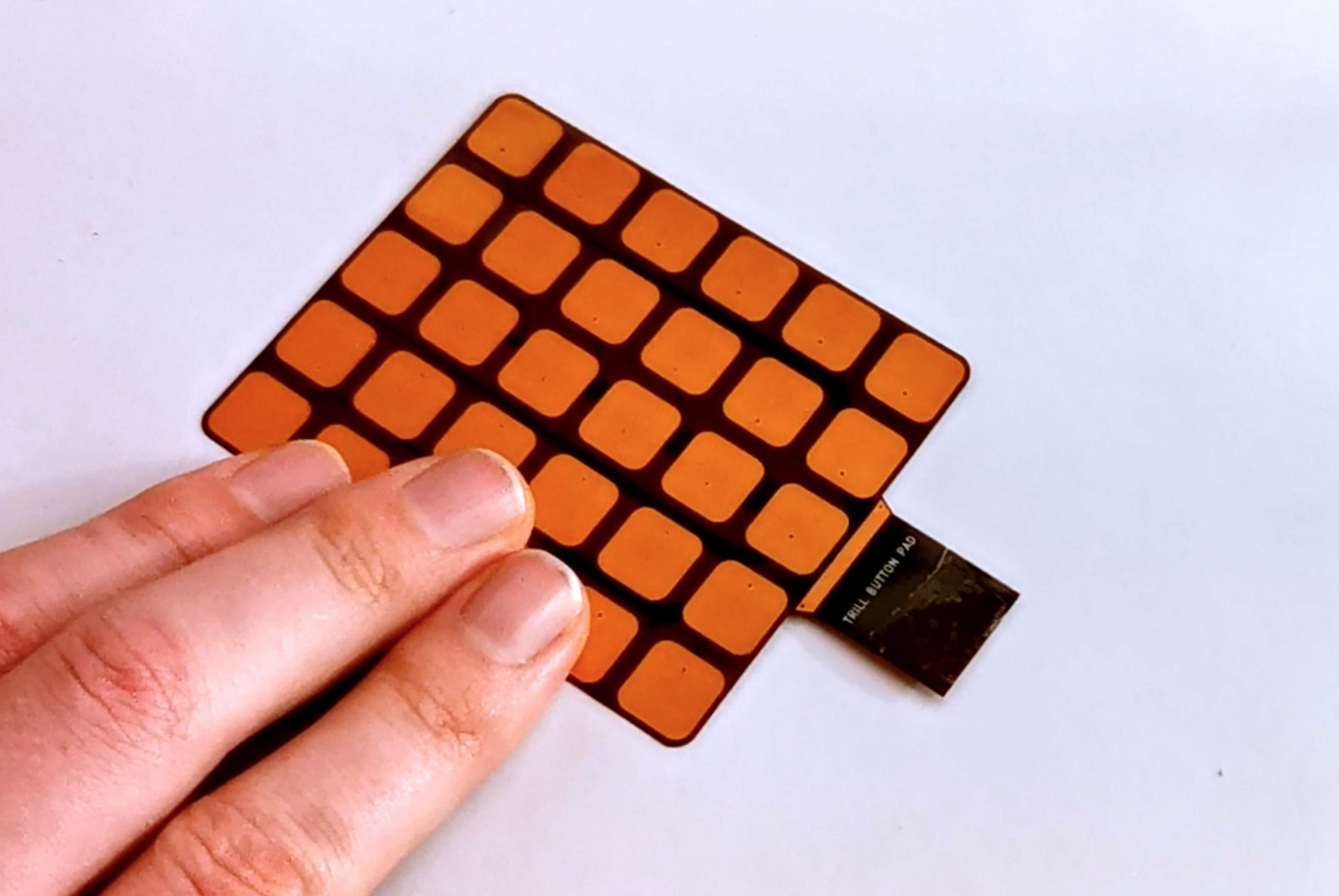
In this tutorial you’ll learn how to design a custom 30-button touchpad for Trill Flex for printing on flexible PCB. We’ll walk you through all the steps in KiCad, from start to finish. Your final product will look like this:
About Trill Flex
Trill Flex is the sixth addition to the Trill family of capacitive touch sensors. Trill Flex’s flexible sensor easily conforms to curves, bends, corners and more, giving you the freedom to create projects with touch surfaces that are virtually any shape.
There are two parts to Trill Flex:
- The base, where you’ll find the Trill chip and a high-density connector
- The flexible sensor, made from flex PCB that attaches to the base via a clip
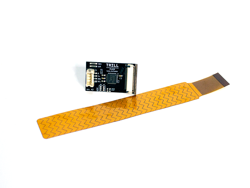
Because the sensor is detachable, you can swap out the default sensor for one of your own designs. There is a myriad of design possibilities for custom Trill Flex sensors, because Trill offers 30 channels of capacitive sensing. Each channel can act as a single sensor, or can be combined in interesting ways - the possibilities are endless.
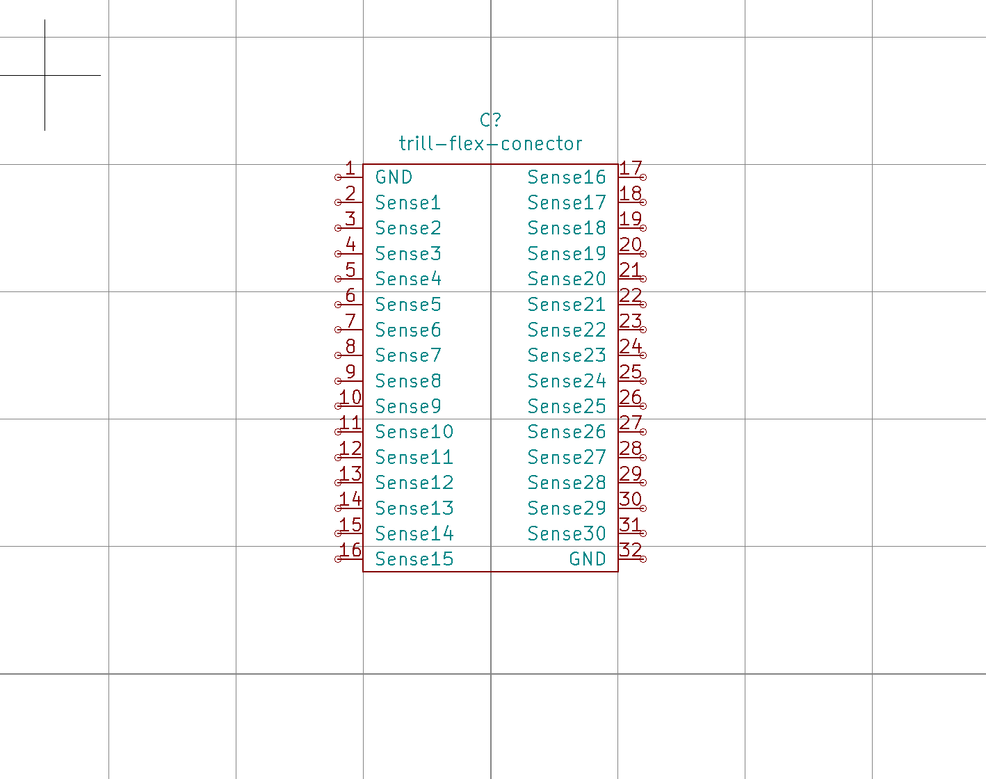
About the Trill connections
The Trill Flex footprint has 32 connections. The outer two connections are both ground, and can be used to connect to a ground plane (we’ll look at this later). On the sensor that comes with Trill Flex you can see the ground is connected to a horizontal strip before the slider begins.
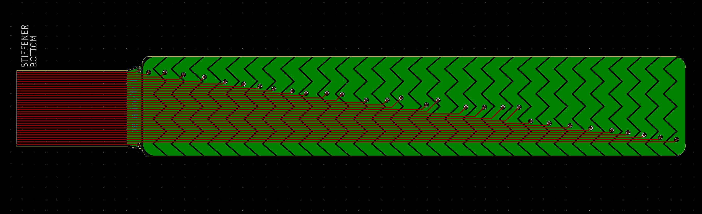
The remaining 30 channels are our capacitive sensing channels. On the included Trill Flex sensor these are connected to each of the zig-zag shaped pads. If you want to see how these pads are designed, you can download the KiCad files for the flex bar PCB here.
In this tutorial we’ll break each of these 30 channels out to 30 touch pads to make a button interface.
A note about flex PCB manufacturing
Though they’ve gotten far more affordable recently, flex PCBs can be quite pricey in small quantities, starting at about $10USD per square inch. We’ve teamed up with OSH Park to offer you flex printing at a discounted rate - every Trill Flex ships with a unique discount code that you can use for $20 off your flex PCB order.
After you draw your polygon in step 8 of this tutorial, we recommend uploading that file to oshpark.com to get an estimate of the final cost.
Set up: Download and install KiCad
This tutorial uses KiCad 5.1. KiCad is a free program for PCB design, and one of the best tools you can learn for creating your own circuit boards, and is available for Windows, Linux or MacOS on the KiCad downloads page.
It’s worth investing some time to get to know KiCad! There are lots of tutorials available online and especially on YouTube, but the KiCad Docs page is a good place to get started if you want to know more.
1. Download the KiCad Trill Flex libraries
We have created footprint and symbol libraries which will provide the basis for designing your own sensors in KiCad. Download the libraries, then move them to a place on your computer where you can find them (such as a folder in your KiCad Libraries directory).
What’s in the library
The folder contains a file for symbol library (trill-flex.lib) and a folder for the footprint library (trill-flex.pretty). The symbol represents the electrical connections of our Flex sensor and is needed for the schematic part of our KiCad project - the schematic is where define all the components that will be included in our circuit, and describe the electrical connections between them.
The footprint library (trill-flex.pretty) contains different footprints for the Trill Flex connector (which will show with the .kicad_mod extension). These footprints represent the part that will be added to your PCB and that actually contains the physical design elements that will be part of our sensor.
2. Load the trill-flex symbols and footprints
Include the symbol library
Go to Tools > Edit Schematic Symbols to open the Symbol Editor. Then, go to Preferences > Manage Symbol Libraries ...
This brings up a dialog box. Click the the small folder icon in the bottom left of the box, which will open a file explorer window. Navigate to the folder containing your download files and select the trill-flex.lib. Click Open.
Your symbols are now loaded! Click OK to close the symbol editor.
Including the footprint library
Return to the main KiCad window. You may have to move the Symbol Editor window out of the way to find it (the main window has KiCad in the title bar with the version number.)
Navigate to Tools > Edit PCB Footprints to open the Footprint Editor (if you can’t see this option make sure you’ve clicked on the main KiCad window).
Then, select Preferences > Manage Footprint Libraries ... Click on the small folder icon on the bottom left. Navigate to your downloaded folder and select trill-flex.pretty, and Open.
Your footprints are loaded! Click OK to close the footprint editor.
3. Set up a new KiCad project
Create a new KiCad project. Return to the main KiCad window. Click File > Create a new project and give it a name. This creates a project file you can see on the left, with pcb and sch files within it. The pcb file is our footprints, and the sch is the scehmatic.
4. Add the Trill Flex symbol to the schematic
Second, we’ll add our symbol to the schematic. Open the schematic by clicking the sch file in the project, or by clicking the schematic button. Select Place > Symbol, and then click anywhere on the schematic. In the search bar, enter trill-flex, the name of our symbol.
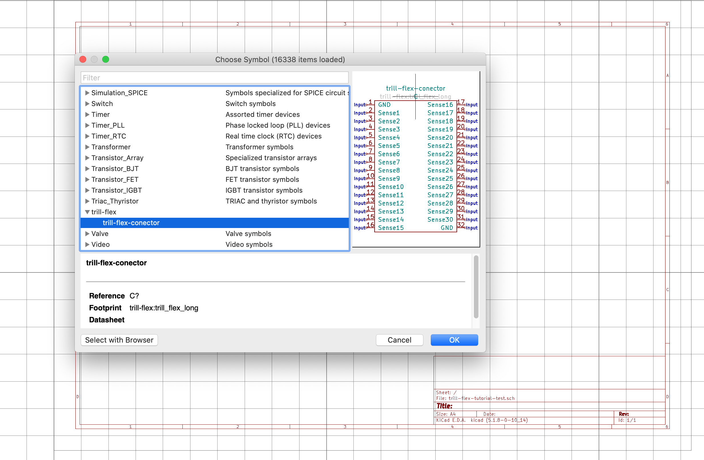
Click on trill-flex in the search result, and you’ll be returned to the schematic. Click anywhere on the page to place the symbol, then save and close the schematic.
5. Add the Trill Flex footprint to the PCB
Open the Layout Editor by clicking the pcb file in the project, or by clicking the Schematic Layout Editor button. Go to Tools > Update PCB from schematic.
You will get a dialog box asking if you would like to Annotate the schematic. Click Annotate, which will open the PCB window again. Click Update PCB. and the footprint should appear under your cursor. Click to place the footprint.
As the footprint explorer window is loading up you will see any load errors reported. If you scroll down to the end of the list and see an error relating to trill-flex then you may need to check your installation of the footprints.
Getting familiar with the footprint
We’ve taken care of the hard part of the sensor design, which is the pigtail lead: a 0.5mm pitch FFC 32-channel cable. This is the part which mates with the connector on the base Trill Flex board.
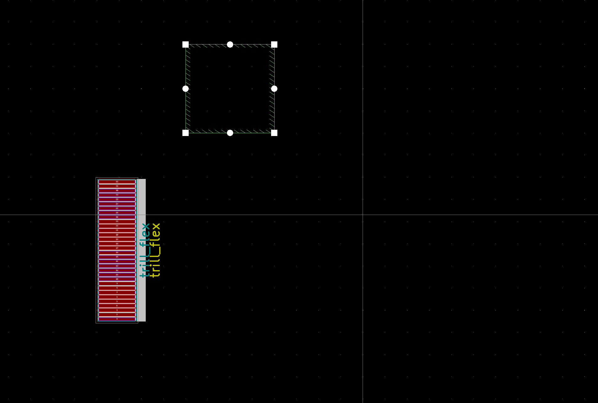
The Trill Flex footprint has 32 individual wires and two sides. One side is the part that make contact with the connector on your Trill Flex board. It can be identified by the footprint title trill_flex_connector_long. We do not need to do anything with this side of the connector - all of the connections we will draw will be with the other side.
It can be easier to work with the footprint when it is oriented in another direction. You can rotate the footprint by clicking on it to select and then pressing the R key. We suggest orienting the connector side of the footprint with the title to left and drawing connections on the right.
6. Draw the pads
Open the PCB file.
First, switch to the bottom layer of our PCB where we’ll do the drawing, called B.Cu. You can see all your layers in a list on the right of the screen, and you can click B.Cu in that list to switch to that layer. You can also use the dropdown menu at the top of the window to switch layers if you prefer.
Next, click the Add filled zones button on the right side of the window (it’s the 7th icon down, but hover over the button if you’re not sure and a tooltip will appear). This mode lets us draw shapes on the PCB by clicking to place corner points.
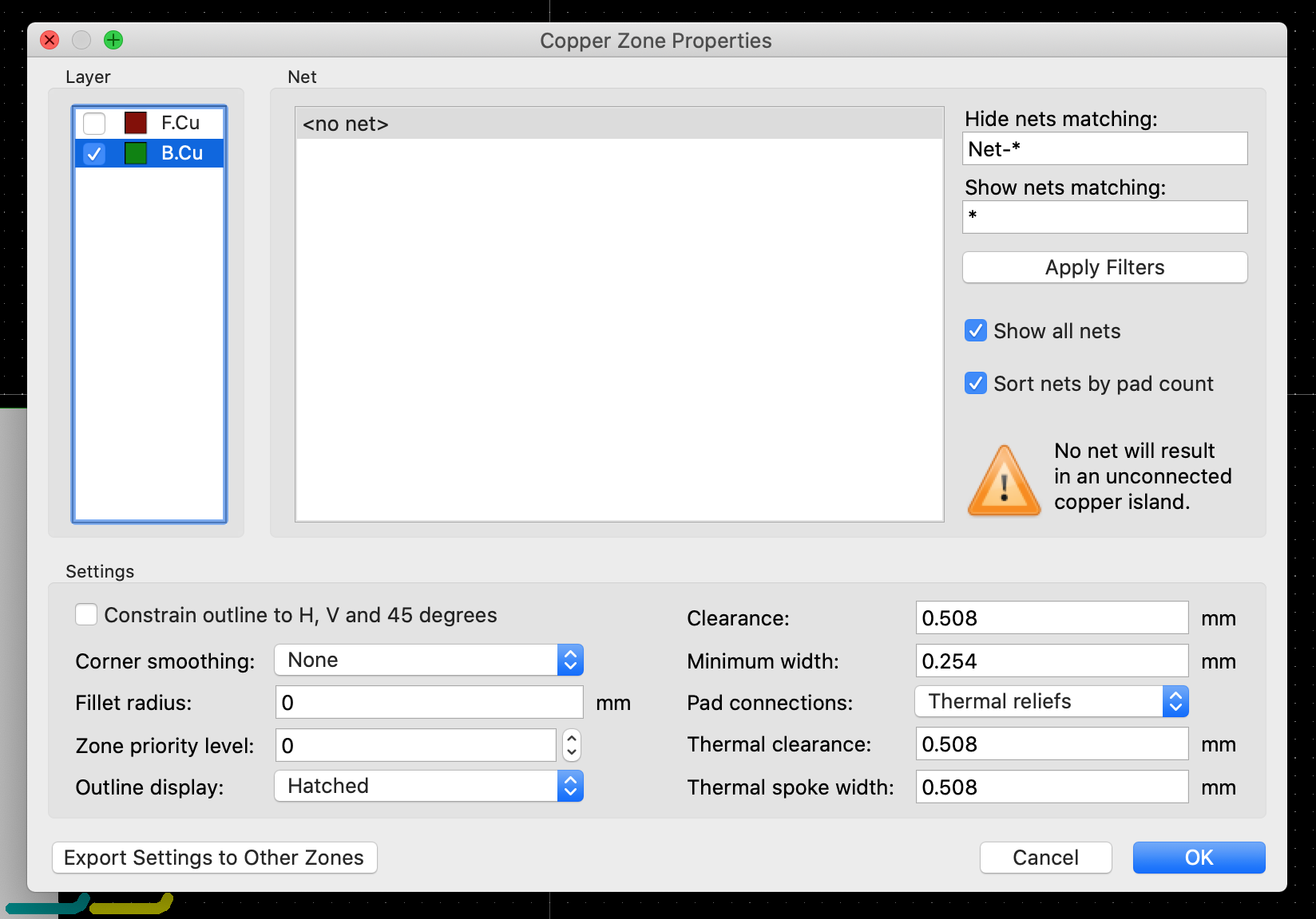
Click on the PCB where you want to start drawing. A settings window will appear, but we’ll just ignore this for now. Confirm you’re on layer B.Cu and click OK.
Pad settings window with bottom layer selected.
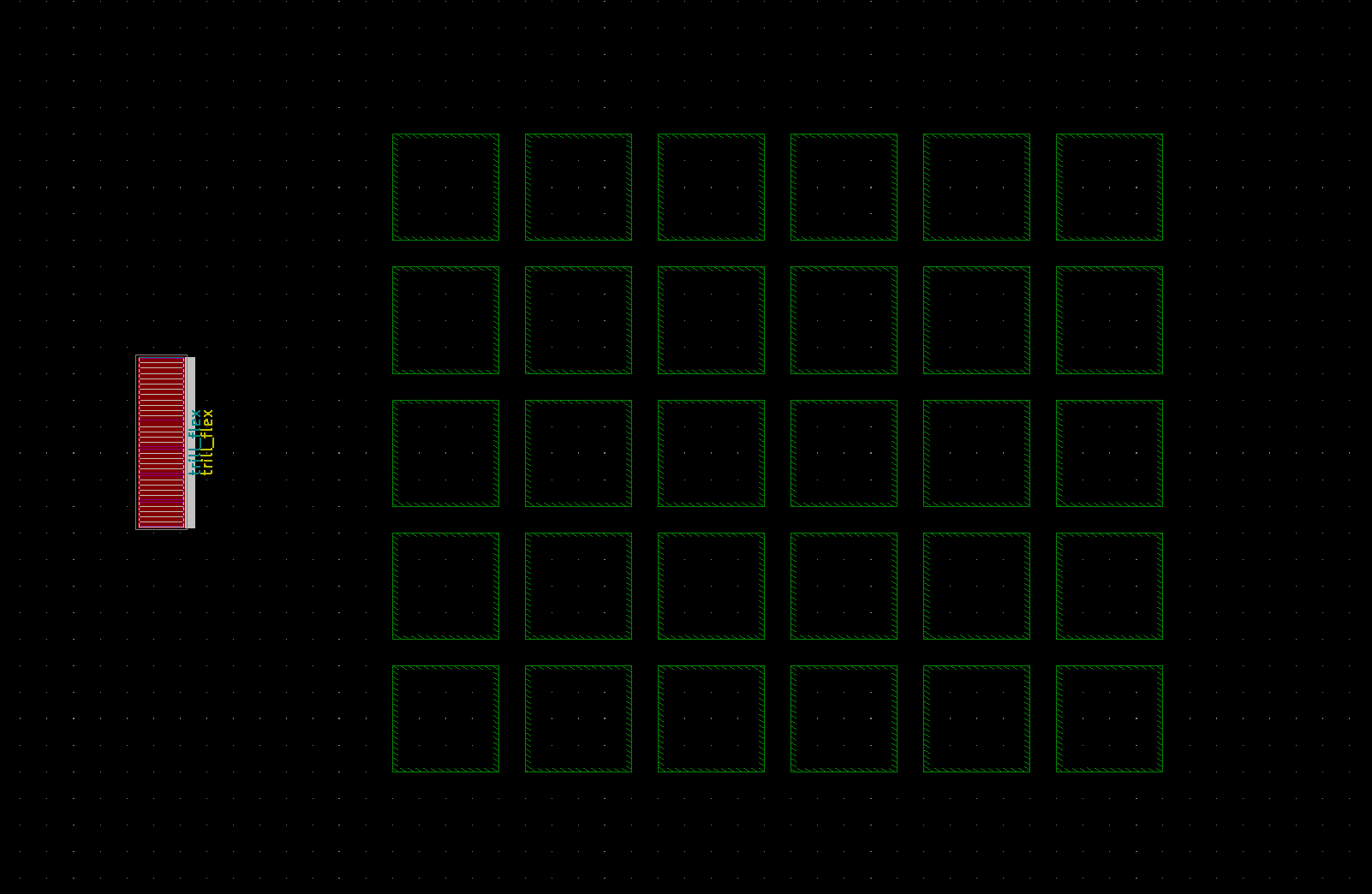
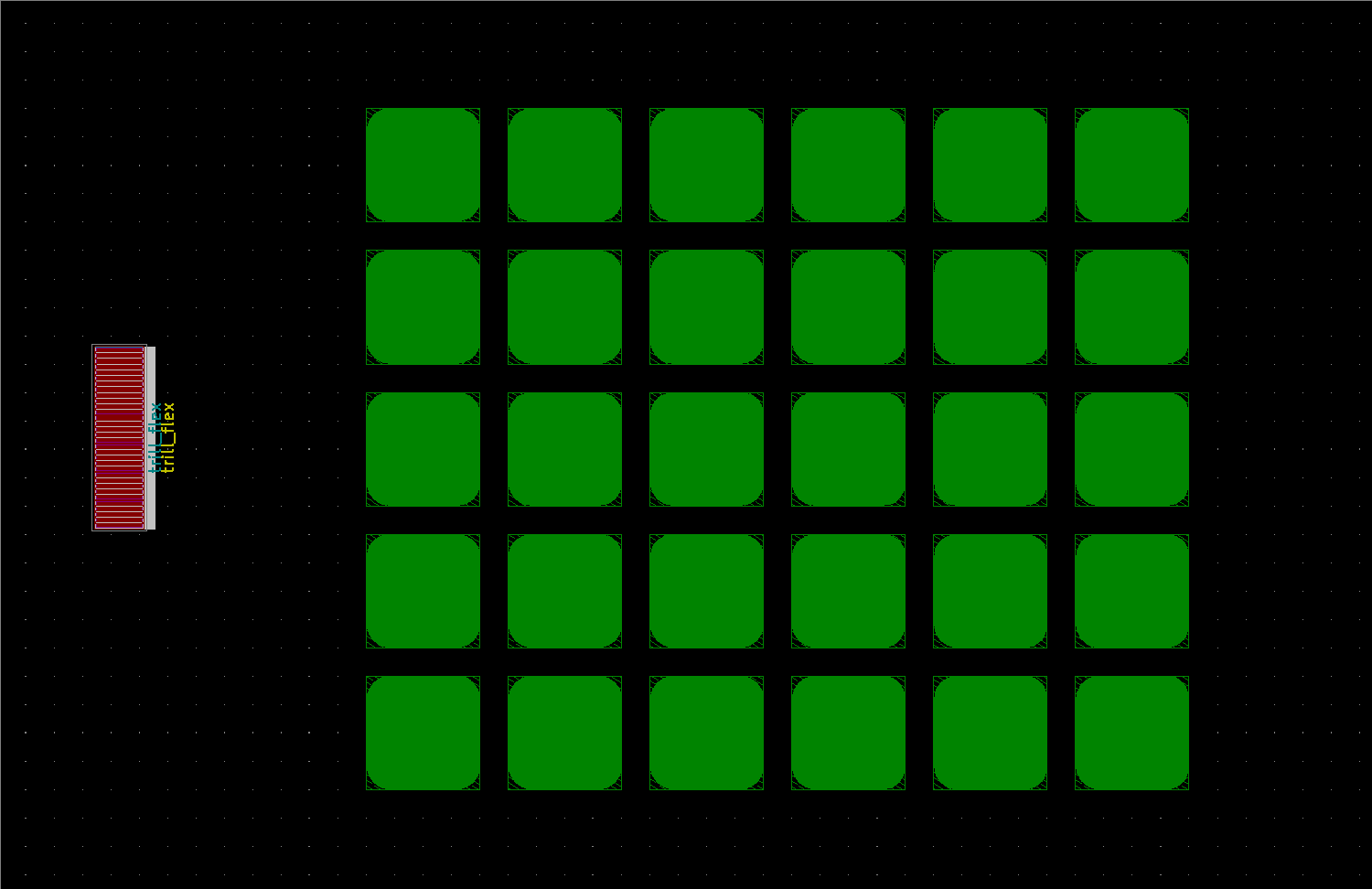
Now we’ll create a 30-button array in the style of an MPC controller, with 30 squares that are 10mm on each side. Change your grid size to 2.5mm with the dropdown menu at the top, meaning each square will be 4 dots wide and 4 dots high. To draw the first square click to place each corner, and then double click to finish the shape.
We can then duplicate this square by switching to Select mode (the cursor icon on the right). Select your square and click Ctrl+C for copy, then Ctrl+V to paste it. Repeat until you have a 6x5 grid of squares. Leave one unit of space (or 2.5mm) between your squares to keep the design compact.
If you need to adjust the grid in KiCad for snapping to it then you can do so via the top menu. Go to View > Grid Settings... Here you can change the size of grid.
Finally, we’ll round the edges of the squares. Double click on a square to open the Settings window. Find “Corner smoothing:” on the bottom left. Select let’s select Fillet, and set the “Fillet radius” field to 2. Click Export Settings to Other Zones to apply these settings to all the other squares. Finally, OK to close the window and see the changes applied.
Ground planes
Adding an additional polygon to your design connected to the two ground channels on the outer edges of the connector can be a good idea as it helps add rigidity to your flex PCB and can also shield connections that are running on the other side of the PCB from registering touches on the other side.
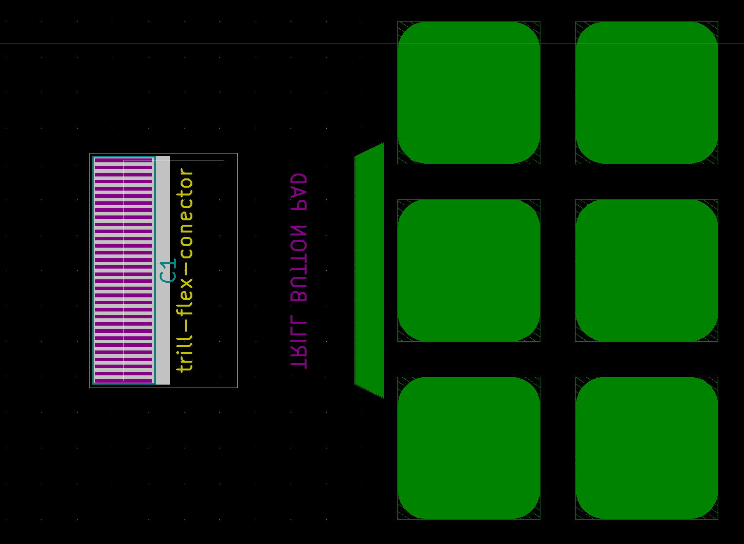
In our design we’ve added a polygon to on the lead of the sensor to add strength at a potential bend point and shield the connections from touch interference. You can see the shape we have drawn above. Depending on your design the ground plane can also be useful for separating different sensing areas, for example multiple sliders.
7. Connect the nets
A “net” is an electrical trace. In this step we’ll add nets from the connector to each of the squares.
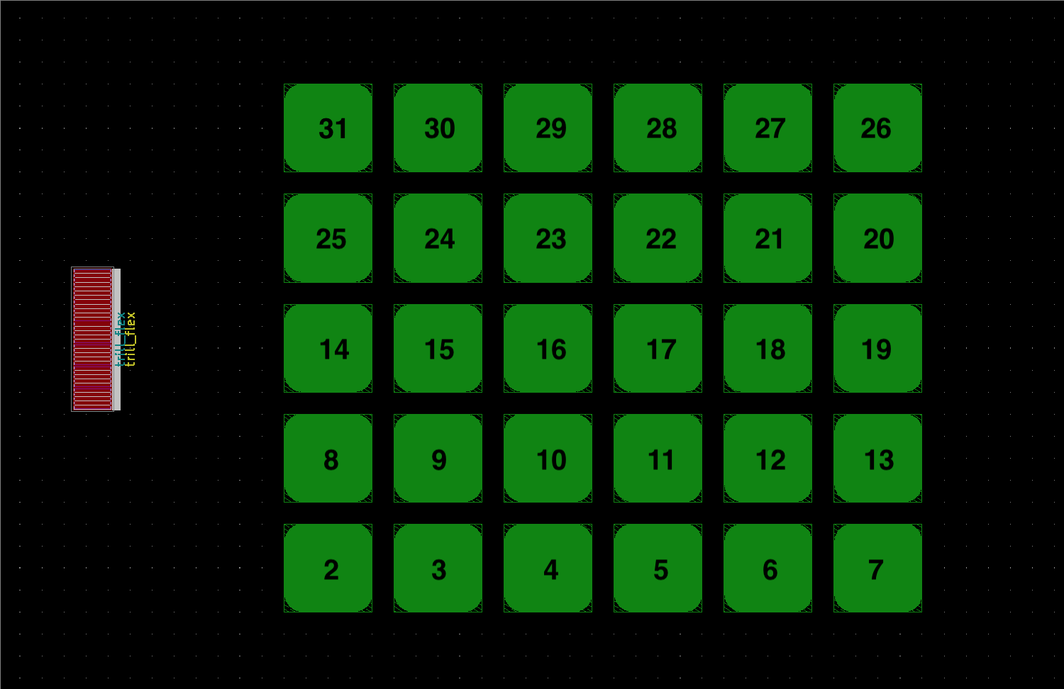
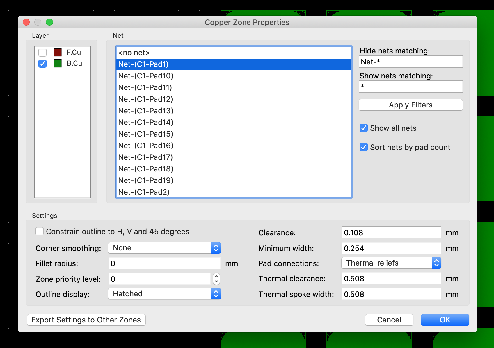
We’ll number the pads from the top left, work right, and go down one row at a time. See the above diagram for numbering. For each pad, double click to open the helper window, and select the correct net for that pad (starting at Net-(C2-Pad2)). You’ll have to click on the squares one at a time and assign them a net number.
Why are our pads connected to nets 2-31? That's because we have 32 pads, and the ones on the outer edges - pad 1 and 32 - are connected to ground.
The ground plane should then be connected to the outer two pads numbered 1 and 32.
8. Make the connections
Now we’ll draw connections from the different pads we have on the connector footprint to each of the square pads we have drawn.
Before doing this make sure that the Trill Flex connector is in the right position for our design. The ideal position for each project will depend on the PCB design, for but for this tutorial place it on the left side with the connectors facing to the left. (If you need to rotate it, select it and press R.)
The connector footprint has 32 connection pads. The outer two connections are both ground and can be used to connect to a ground plane. The remaining 30 channels are your capacitive sensing channels. In our case we have added an additional pad across the connector which we connect to ground.
We can route electrical connections between the flex connector footprint and the squares using the Route tracks tool on the right hand side (looks like a green line, 5th icon down). We want to route on the top copper layer so make sure we’re on F.Cu. To begin routing click on the pad of the connector (remember to start with Pad 2 because Pad 1 will go to ground!). You can then draw out the path of the trace by clicking to place a bend point.
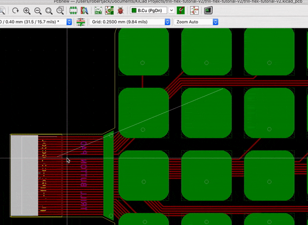
Our traces are on the top layer of the PCB, but we need to make a connection with the pad we drew on the bottom layer. To do this we’ll place a via, or a hole through the PCB that allows us to route traces from one side to the other.
To place a via while routing type v, and click to place the via. You will now be on the other side of the PCB, on the bottom layer. There is just one final connection necessary, from the via to our pad. This can be done by just double clicking the via after placing it.
Though there are some conventions about drawing traces, everyone does this a little differently. You can follow our diagrams exactly, or define your own paths.
9. Draw an outline
Now we need to define the overall shape of the sensor. This outline has to include the connector as well as our pads.
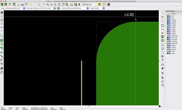
To draw the outline of your board, we need to add a polygon on the Edge.Cuts layer. Click the Add graphic polygon button on the right (looks like a blue shape, 7th from the bottom). Then, select the Edge.Cuts layer. Define your outer shape by clicking to add points. We have opted to leave 0.5mm where possible between the sensor pads and outline. Refer to the diagram above for a good shape, but make sure that your connector neck has a diagonal cut where it meets the pads (right angles on flex PCBs can weaken and snap over time).
10. Run the design rules and electrical check
The design rule check, or DRC, confirms that everything is connected correctly. To run it click on the ladybird icon on the top menu bar, and click ‘Run DRC’ in the dialog box. If there are any issues with your design, for example unconnected traces, then this will show up as a red arrow on the PCB to highlight where the problem is. You can return to your PCB and correct the issue, and rerun the DRC until you can get through without any errors.
At this point another good check to perform is to print your design on paper to make sure that the dimensions are all as expected. In KiCad you can go to File > Print... and then select the layer which you would like. Make sure the scale is set to 1:1.
11. Generate the file for manufacturing
There are several companies that offer flex PCB manufacturing, but we’ve teamed up with OSH Park to offer discounted flex printing for Trill Flex enthusiasts - each Trill Flex comes with a unique OSH Park discount code for $20 off the final cost.
To place an order with OSH Park
On the front page of oshpark.com click Browse for files and select the pcb file from your project. You’ll get a nice preview of your board as it will be printed. If you see the warning “nothing present on mask stop bottom layer (check what this actually is)” you can ignore that, unless you are expecting to have something there. This warning is just telling us that there is no exposed copper on the bottom layer which is expected in this design.
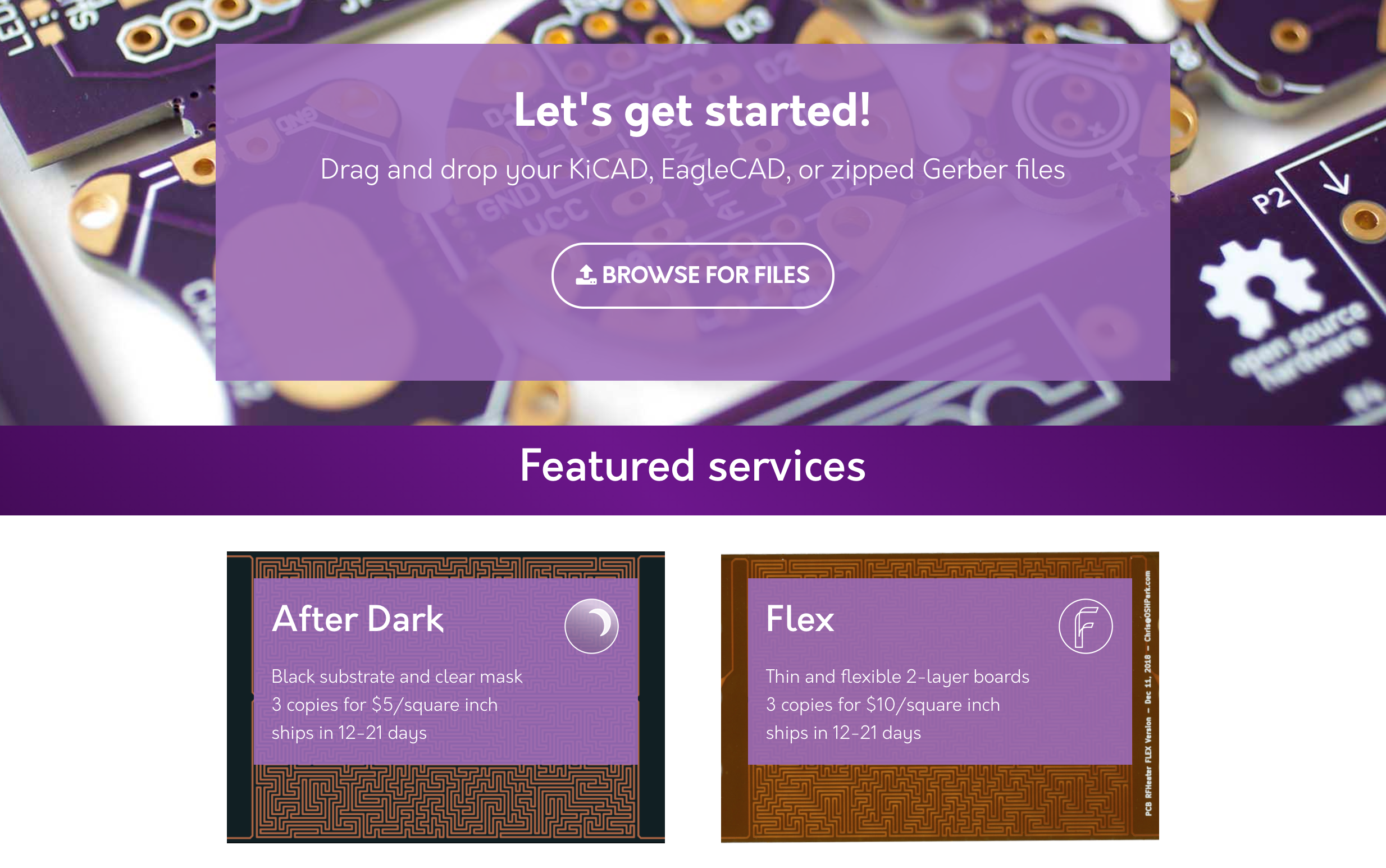
On the next page select Flex PCB from the options available, and enter your coupon code. You’re now ready to place your order with a $20 discount!
Exporting files for other manufacturers
Other manufacturers will expect you to provide them with gerbers files which are a recognised standard for manufacturing PCBs. To export your project as a gerbers you need to do the following:
Select the Plot icon from the toolbar on the top menu. A window will popup asking you about the layer you would like to export as part of the Gerbers. Generally the default settings will be fine for generating the Gerbers file. You just need to give an Output Directory and then click on Plot which will generate the Gerber files in the folder given. Most other manufacturers will allow you to upload these files as a .zip on their website.
Flex PCB settings
When manufacturing your Flex PCBs at other PCB houses than OSH Park you will likely need to set the thickness of the PCB and various other parameters. Here are some of our recommendations for setting which work.
At the end of the sensor you are aiming for overall thickness of 0.3mm +/-0.05mm to make a good connection with the Flex base board. We have used the following settings with other PCB House with great results. Note that you will need to correspond with the PCB house to understand how they expect the stiffener to be indicated on the PCB design files.
| Thickness of the Flex PCB: | 0.15 mm |
| Thickness of the stiffener: | 0.2 mm |
| Stiffener location: | TOP |
| Stiffener material: | PI (polyimide-stiffener) |
12. Get your sensor ready to use!
Congratulations, you have just received your first custom flex sensor design! There’s one last step before you can start using your new sensor.
Before connecting your sensor to the Trill Flex board it’s necessary to add a small piece of tape to the connector to make sure that it fits snugly into the board’s clip (otherwise it can move around). Take a look at the sensor that came with Trill Flex, and you’ll see a small piece of stiffener plastic. A layer of sellotape or two layers of Captan tape works a treat. Note that it’s better to have the tape finish before the edges of the sensor rather than hang over.
Now you are now ready to test your sensor out! Plug the sensor into the flex connector board. Run flex-settings as a start. Once this project is running you can launch the GUI and adjust the settings to be optimal for your layout.
You may find that you are getting no visible readings when you first launch this project but do not fear! Try changing the prescaler value and resetting the baseline to see the effect. We find a prescaler value of 4 or 5 works best for the flexible bar sensor we ship as default with Trill Flex.